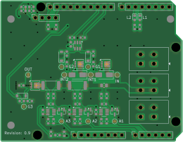
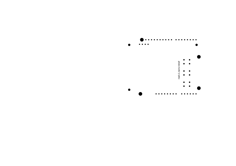
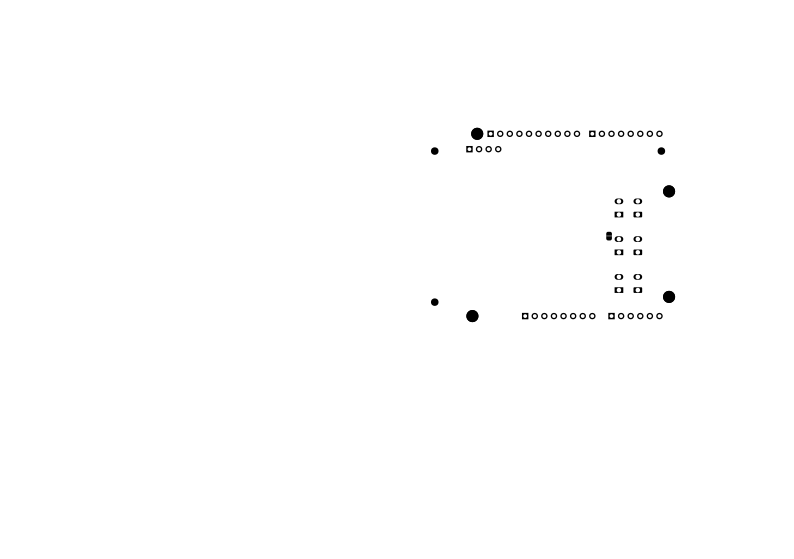
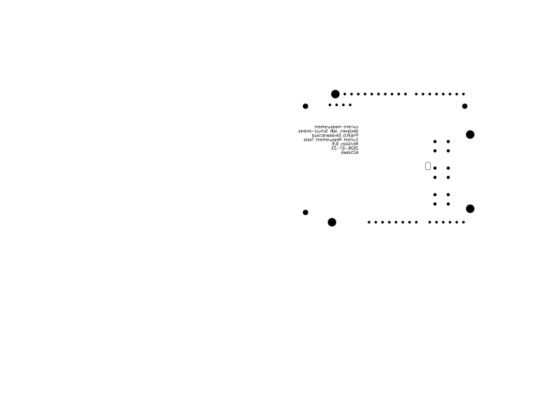
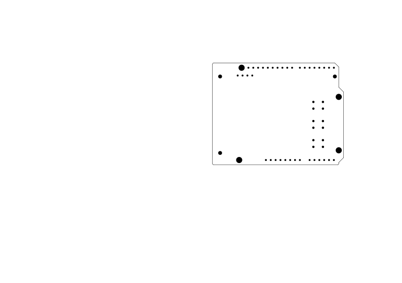
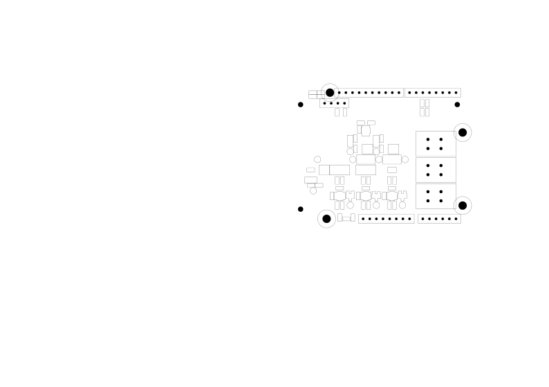
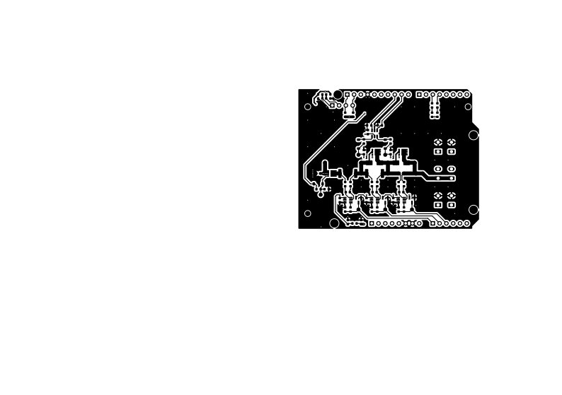
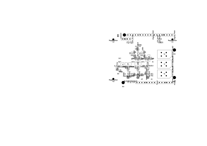
This PCB measures a device's current consumption over a wide dynamic range, from microamps to amps. It is intended for automated hardware testing, where the same device may alternate between very low-power sleep states and short high-current activity.
The current path contains three shunt resistors:
Two MOSFETs bypass the 100 Ω and 1 Ω shunts when their sensitivity is no longer required. Each shunt has its own INA190 current-sense amplifier and a separate ADC output, so the controller can select the appropriate range while still observing the other measurement channels.
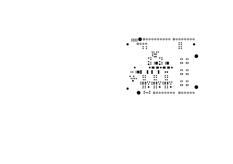
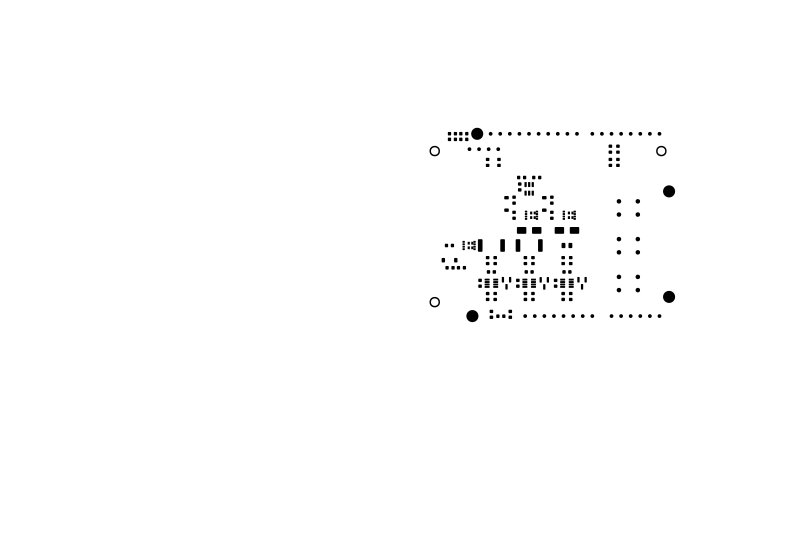
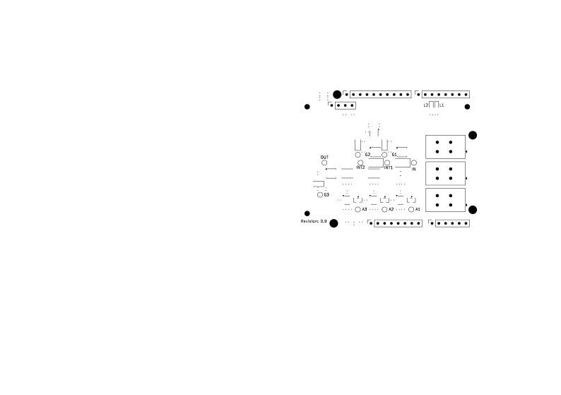
This document describes schematic and layout revision 0.9.
The PCB is inserted into the current return path between IN and OUT. Current flowing from IN to OUT produces a voltage across each active shunt:
V_SHUNT = I_LOAD × R_SHUNT
The corresponding INA190 amplifies this voltage:
V_ADC = V_REF + I_LOAD × R_SHUNT × GAIN
In this design, all INA190 REF pins are connected to ground, so:
V_ADC ≈ I_LOAD × R_SHUNT × GAIN
The implementation is therefore unidirectional. Positive current produces a positive ADC voltage. Reverse current cannot be measured accurately because the amplifier output cannot swing below ground.
The PCB is designed for low-side current sensing. OUT, the controller ground and the PCB ground must remain at approximately the same potential for the ground-referenced MOSFET gate drive to work correctly.
| Range | Shunt | Amplifier | Gain | Sensitivity | Approx. full scale |
|---|---|---|---|---|---|
| Low current | 100 Ω | INA190A5 | 500 V/V | 50 mV/µA | 65.2 µA |
| Medium current | 1 Ω | INA190A5 | 500 V/V | 0.5 V/mA | 6.52 mA |
| High current | 10 mΩ | INA190A4 | 200 V/V | 2 mV/mA | 1.63 A |
The full-scale values use the INA190's specified positive output swing of approximately:
V_OUT,max = V_S - 40 mV = 3.26 V
with a 3.3 V analog supply.
These are ADC/amplifier full-scale limits, not necessarily the absolute safe current limits of the PCB. Connector ratings, copper temperature rise, MOSFET dissipation and shunt temperature must also be considered.
Q3 bypasses the 100 Ω shunt and Q2 bypasses the 1 Ω shunt.
The control signals pass through an SN74LVC2G04 inverter, so a low control input turns the corresponding bypass MOSFET on.
GATE1 |
GATE2 |
Q3: 100 Ω bypass | Q2: 1 Ω bypass | Intended range |
|---|---|---|---|---|
| 1 | 1 | Off | Off | Low-current range |
| 0 | 1 | On | Off | Medium-current range |
| 0 | 0 | On | On | High-current range |
| 1 | 0 | Off | On | Not normally used |
R15 and R16 pull the inverter inputs low. Once the 3.3 V logic supply is present, both MOSFETs therefore default to on and the PCB starts in the least sensitive, highest-current range.
A sensible autoranging strategy is:
The INA190 typically settles to within 1% after a current step in about 30 µs. After a differential overload, recovery can take approximately 80 µs, so a firmware delay of roughly 100 µs is a reasonable conservative starting point and should be verified on the assembled PCB.
The design uses two INA190 gain variants:
Relevant INA190 properties include:
| Parameter | Value |
|---|---|
| Supply range | 1.7 V to 5.5 V |
| Input common-mode range | -0.2 V to +40 V |
| Input offset voltage | ±15 µV maximum |
| Input bias current | 0.5 nA typical, 3 nA maximum |
| Common-mode rejection | 132 dB minimum |
| Quiescent current | 48 µA typical, 65 µA maximum |
| INA190A4 gain error | ±0.3% maximum |
| INA190A5 gain error | ±0.4% maximum |
| INA190A4 bandwidth | 33 kHz typical |
| INA190A5 bandwidth | 27 kHz typical |
| Current-step settling time | 30 µs typical |
| Differential-overload recovery | approximately 80 µs |
The very low input bias current is especially useful for the 100 Ω range because the amplifier does not significantly load the shunt.
The INA190's maximum input offset corresponds to the following input-current uncertainty before calibration:
| Range | Calculation | Offset-equivalent current |
|---|---|---|
| 100 Ω | 15 µV / 100 Ω | 150 nA |
| 1 Ω | 15 µV / 1 Ω | 15 µA |
| 10 mΩ | 15 µV / 10 mΩ | 1.5 mA |
The INA190 also has a small positive zero-current output when REF is grounded. The maximum specified value is 9 mV for the A5 and 4 mV for the A4. Each channel should therefore be zero-calibrated in firmware.
A practical calibration stores at least:
Each INA190 input uses two 33 Ω series resistors and a 22 nF differential capacitor.
The differential cutoff frequency is approximately:
f_C = 1 / (2π × (R_IN+ + R_IN-) × C_DIFF)
    = 1 / (2π × 66 Ω × 22 nF)
    ≈ 110 kHz
This cutoff is above the INA190's own 27 kHz or 33 kHz small-signal bandwidth, so the amplifier remains the dominant bandwidth limitation.
The input network is still useful because the INA190 uses a capacitively coupled input stage. TI notes that sufficiently large and fast shunt-voltage transients can disturb the output even when the transient frequency is above the nominal amplifier bandwidth. The differential RC network attenuates these spikes before they reach the amplifier.
The 22 nF capacitor should be placed close to the INA190 input pins, and both sense traces should be routed as a matched Kelvin pair from the shunt pads.
Each amplifier output is followed by a 330 Ω series resistor and a 2.2 nF capacitor to ground.
Its nominal cutoff frequency is:
f_C = 1 / (2π × 330 Ω × 2.2 nF)
    ≈ 219 kHz
This is much higher than the INA190 bandwidth, so this RC network is not the main bandwidth-limiting or anti-alias filter. Its main functions are:
The INA190 specifies a maximum direct capacitive load of 1 nF without sustained oscillation. The 330 Ω resistor isolates the amplifier from the 2.2 nF capacitor.
For sampled measurements, the ADC should run sufficiently faster than the useful analog bandwidth. Oversampling followed by digital low-pass filtering and decimation can then define the final measurement bandwidth. The analog response is not a brick-wall filter, so additional filtering may still be needed in environments with strong switching interference above half the ADC sampling frequency.
Q2 and Q3 are CSD16340Q3 25 V N-channel MOSFETs driven from 3.3 V through 33 Ω gate resistors.
Relevant specifications are:
| Parameter | Value |
|---|---|
R_DS(on) at V_GS = 2.5 V |
6.1 mΩ typical, 7.8 mΩ maximum |
R_DS(on) at V_GS = 4.5 V |
4.3 mΩ typical, 5.5 mΩ maximum |
| Total gate charge at 4.5 V | 6.5 nC typical, 9.2 nC maximum |
| Drain-source voltage rating | 25 V |
The datasheet does not provide a tabulated R_DS(on) specification at exactly 3.3 V. Because the gate drive is above the rated 2.5 V point, the 7.8 mΩ maximum at 2.5 V is a conservative design value.
The MOSFET resistance is not part of the measured shunt voltage, but it contributes to the voltage dropped in the DUT return path.
Approximate total current-path resistance is therefore:
| Range | Approximate path resistance |
|---|---|
| Low | 100 Ω + 1 Ω + 10 mΩ = 101.01 Ω |
| Medium | Q3 + 1 Ω + 10 mΩ ≈ 1.016 to 1.018 Ω |
| High | Q3 + Q2 + 10 mΩ ≈ 22.2 mΩ typical, 25.6 mΩ conservative |
The high-current range therefore has more burden than the 10 mΩ shunt alone. At 1 A, the total return-path drop is approximately 22 to 26 mV before PCB trace and connector resistance.
R_DS(on) rises as the MOSFET warms up, so the high-current burden voltage should be measured on the assembled PCB under realistic thermal conditions.
The theoretical current corresponding to the resistor's rated power is:
I = sqrt(P / R)
  = sqrt(0.125 W / 100 Ω)
  ≈ 35 mA
This is far above the intended 65 µA measurement range, but the resistor can still be overstressed by a sudden high-current event before the bypass MOSFET turns on. Firmware should therefore avoid enabling this range unless a lower-sensitivity channel has already confirmed that the current is safe.
The nominal power-limited current is approximately:
I = sqrt(2 W / 1 Ω)
  ≈ 1.41 A
The INA190A5 output saturates at roughly 6.52 mA in this range, long before the resistor reaches its power rating.
The amplifier and ADC reach full scale at approximately 1.63 A. The resistor itself is rated for substantially more current, but the complete PCB current rating may be lower.
The INA190 amplifiers use the filtered +3.3VA rail.
The analog rail is derived from +3V3 through a Murata BLM18AG601SN1D ferrite bead with:
A 1 µF capacitor is placed on each side of the bead, and each INA190 has its own local 100 nF bypass capacitor. This network isolates high-frequency digital noise from the current-sense amplifiers.
The ferrite bead does not create a precisely defined low-pass cutoff frequency. Its impedance is strongly frequency-dependent and interacts with the surrounding capacitors and PCB parasitics.
The useful analog bandwidth is mainly set by the INA190:
The ADC sampling frequency should be comfortably above twice the highest useful analog frequency. Sampling faster also permits digital low-pass filtering and decimation.
The required sampling rate depends on the intended measurement:
Digital filtering cannot remove signals that have already aliased into the sampled band. If significant energy reaches the ADC above half the sample rate, either increase the sample rate or add stronger analog filtering.
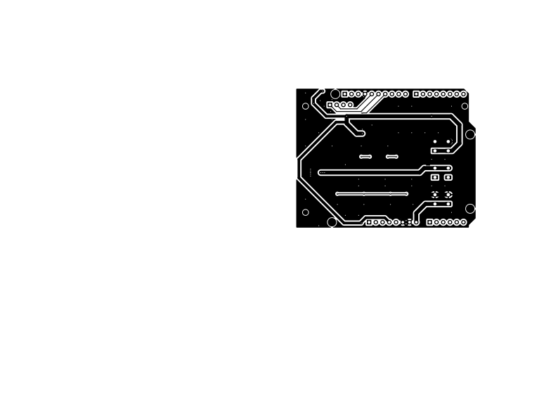
Measurement accuracy depends strongly on PCB layout.
The 10 mΩ range is especially sensitive to layout. One milliohm of unintended shared copper would produce a 10% error relative to the nominal shunt value.
REF pins are grounded.